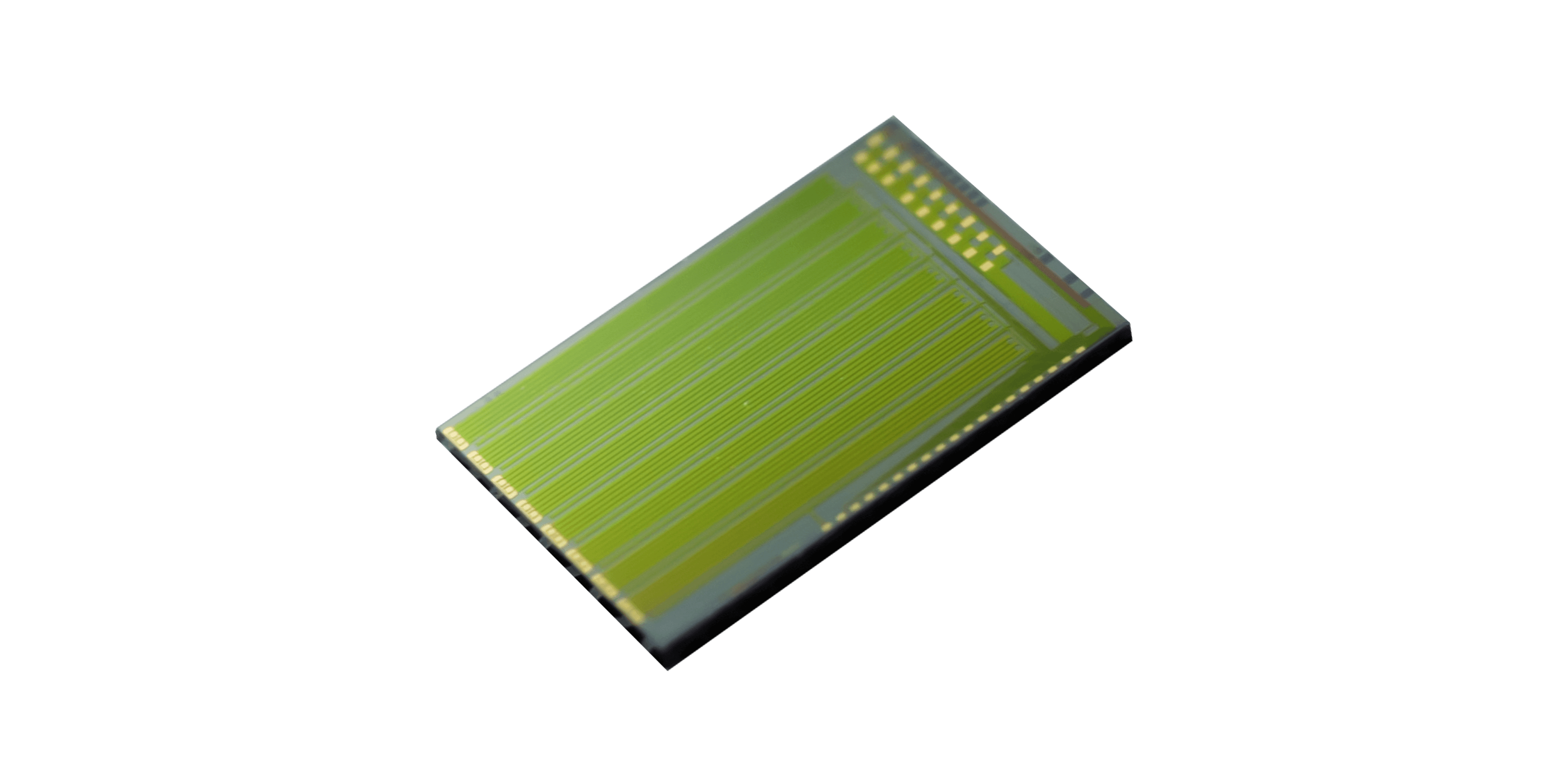
A communication module becomes smaller when its optical, electrical, thermal, and mechanical functions are partitioned intelligently. Shrinking a die while leaving difficult fiber alignment, bulky drivers, or complex bias circuitry outside the package may move space rather than save it.
They therefore assess compactness at the module level, where every interface contributes to size and cost. Higher port density creates a linked set of constraints. More channels must fit near the switch or transport platform, yet each channel still needs adequate optical power, signal quality, cooling, test access, and serviceability.
An efficient design is not defined by package size alone; it is the arrangement that delivers required capacity without creating disproportionate energy or production penalties. TFLN chips are relevant because thin-film lithium niobate can support high electro-optic bandwidth with comparatively low drive voltage.
Published options address 800G, 1.6T, and 3.2T module architectures. They use those specifications as inputs to a full design model rather than assuming that one strong device parameter automatically produces a compact finished product.
Compactness Starts with the Partition of Functions
Module architecture begins with channel count and modulation format. Optical chips can combine several high-speed paths on one substrate, reducing the number of discrete alignments and interconnects. A DR8 device, for example, places eight lanes within one product concept.
That integration may simplify assembly, although the package must still preserve uniform RF and optical performance across every lane. Within that architecture, TFLN chips can serve direct-detection or coherent designs. The direct-detection products emphasize multiple intensity-modulation channels, while coherent variants add in-phase, quadrature, and polarization functions.
They select between them according to reach, spectral efficiency, receiver complexity, and interoperability targets, not according to which format appears more sophisticated. Physical layout should be reviewed before the die is frozen.
Fiber-array pitch, edge-coupling geometry, RF pad placement, ground return, heat paths, and control connections all influence the final footprint. They ask the chip and packaging teams to exchange models early because a compact die can become difficult to assemble if the surrounding interfaces compete for the same limited space.
Electrical and Optical Budgets Define Real Efficiency
Low drive voltage can reduce the output swing demanded from the electrical driver, which may lower power and ease signal-integrity design. One 3.2T DR8 specification lists differential half-wave voltage below 1.5 V, while a 70 GHz 1.6T DR8 or 800G DR4 product is below 2 V.
These values must be interpreted with the selected operating point and waveform. Insertion loss determines how much laser power remains for transmission and receiver margin. The listed multilane optical chips include coupling in a stated figure below 14 dB, whereas a bare intensity-modulator die is specified below 5 dB.
They keep these boundaries separate, then add connector, waveguide, splitter, and aging allowances to form a transparent optical budget for the complete module. Bandwidth also affects efficiency because insufficient response may force higher electrical swing or heavier digital equalization.
With TFLN chips spanning 70 to 110 GHz in the published portfolio, they match the response to symbol rate and packaging capability. Excess bandwidth is not free if it raises cost, test difficulty, or sensitivity without improving the required link margin.
Manufacturing Readiness Determines Whether Density Scales
Density is commercially relevant when manufacturing yield remains acceptable. Multi-channel products can concentrate value in one die, but a defect or coupling problem may affect several lanes at once. They request wafer-level screening data, lane-uniformity information, assembly tolerances, and clear criteria for repair or rejection before estimating volume economics.
Optical chips also change test strategy. Parallel electrical stimulus, calibrated optical receivers, automated bias control, and fiber-array handling may be needed to preserve throughput.
They estimate test time per unit and identify which parameters can be screened at wafer level, after packaging, and at final module test. This prevents hidden capital requirements from appearing late in the program. Supply planning completes the readiness review. For TFLN chips, they examine substrate availability, fabrication capacity, package partners, lead-time sensitivity, and process-change control.
A compact architecture can become operationally fragile when one specialized step has no recovery plan. Second-source options may involve compatible interfaces rather than identical internal designs. Mechanical efficiency should include assembly access and repair strategy.
A very dense layout may save board area but make fiber cleaning, electrical probing, or component replacement impractical. They review these activities with manufacturing and service teams before accepting the footprint as an operational improvement.
Their preferred development path starts with a module-level digital model, proceeds through package prototypes, and ends with link testing under temperature and production variation. At each stage, they track volume, power, loss, error margin, yield, and assembly time together. The resulting trade space is more useful than an isolated claim about chip size.
Compact optical modules will continue to support denser switching and transport equipment, but efficiency must remain measurable. They consider watts per transmitted bit, usable ports per faceplate, optical margin, manufacturing throughput, and replacement effort.
A balanced design may occupy slightly more space while providing substantially improved lifecycle performance. Compactness is a module-level result, not a die-area claim. Testing Liobate optical chips inside representative driver, coupling, thermal, and service layouts shows whether a smaller footprint also preserves yield and maintainability.
